Tips For Creating Your Own Custom Material in Substance Designer
Marco Vitale gives us an extensive breakdown of how to do some hard-surface modeling in Substance Designer, as well as how to create emissive elements in a custom material.
Marco Vitale gives us an extensive breakdown of how to do some hard-surface modeling in Substance Designer, as well as how to create emissive elements in a custom material.

Marco Vitale is a german lighting designer for theatre with over 10 years of experience in the field of lighting. Since the theatre is quite an old form of art, the methods are too. A few years back Marco started to develop the lighting for his shows in a 3D-Lighting software called Capture Sweden.
Over time, Marco's interested shifted from theatre lighting, to creating models in 3D and more recently to the texturing and material creation - he was fascinated by what a huge impact the right material can have on the realism of a 3D render. So a little over a year ago Marco bought a Substance license and played around with it a little bit and got really addicted to that amazing piece of software. From that point he tries to create all his materials with Substance Designer.
In this breakdown Marco shows us how to do some hard-surface modeling in Substance Designer, as well as how to create emissive elements in a material.
Sometimes it’s just a 10 seconds brainstorm, sometimes it’s a long way to go. I usually have the best ideas in the most inopportune moments and often when I sit in front of the computer these ideas have completely vanished. I created an empty folder on my dropbox called “ideas and references”. Whenever I have an idea, I take a photo with my phone, record a memo or write a little note and upload it to that folder.
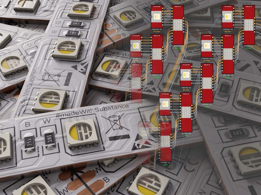
So now, when I sit in front of the computer and want to start a new material I go through this folder and the item which jumps right into my face gets its chance. The idea of doing an LED-Stripe sat there for almost two years - I shot a few photos at work, while the technicians assembled them into a stage prop.
One of the most important steps before jumping into the real fun is collecting references. Most of the time I take very few, around 3 to 5 images, because I don’t want to stick to these too much. But with this material I wanted to create it as true to the original as possible, so I needed a lot more references.

I collected images, manufacturers drawings, I even took a small piece of LED-Stripe and disassembled it - I had the rare opportunity to have my reference lying next to my Mousepad.
Before I start creating a material, I usually try to divide the material into its basic elements. For the LED-Stripe that was the PCB the copperband which holds all the parts; the small resistors which are sitting between the LED-Chips and, of course, the main actor - the LED-Chip. Every element of this material has its own difficulties and challenges which I wanted to address.
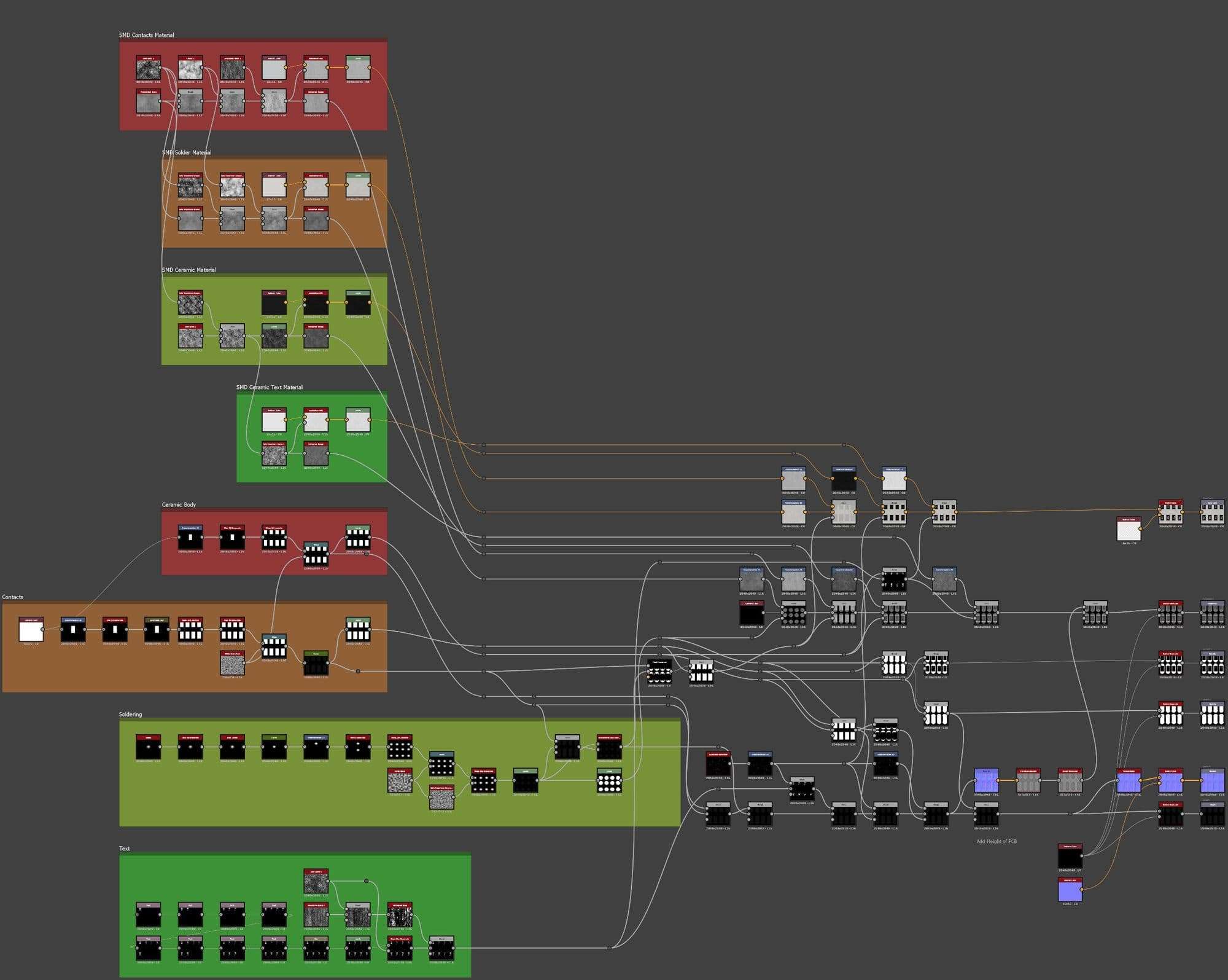
I like my graphs very organised, so I usually create subgraphs for all the main elements. I expose a few parameters, which I want to alter in the main graph, to keep a good overview so as not to end up in a spiderweb of nodes. In this breakdown I will go through the main steps focusing on the tricky parts of all the elements.

My workflow in Substance Designer is always the same. Working from the height to the colour, normal, roughness and metallic maps. But before starting with the Height-Map I had to choose the right scale, because the realism of that material will highly depend on the layering of different elements, the real height is very important.
So I chose a value of 1 corresponding to 10mm in real scale for the height and and started with a X- and Y-Dimension of 100mm x 100mm. But the stripe I had for reference was 84mm x 12mm, so I had to use another scale for the X and Y, to get a tileable material. Now my new scale factor was a bit ugly.
1 / 0.84 = 1.1904761904761904761904761904762
I thought, I’d never get the scale right to be tiling but after calculating the Y-Dimension it accidentally worked out to be a whole number. So the tiling of my material would be 1 x 7.
1 / ((1 / 0.84) * 0.12) = 7
Besides, I created all the elements with the highest scale possible, to have simple numbers, and apply the scale at the end. For this I built some small utility graphs, to apply the right scale and tiling.
The PCB is a thin copperband, with conductor tracks connecting the soldered parts of the strip, the height-map is defined by these connections.

The most exciting thing about the PCB were the quite complicated shapes. So I was searching for a solution to create complex shapes, without using an SVG-Node and stumbled over a QuickTip by Clark Coots on Artstation. In his Tip he is using a Gradient Linear 1 to basically draw almost every shape with the help of the Curve-Node.

The Gradient Linear 1 gets rotated 90 degrees and then subtracted from the result of the Curve-Node and the Levels-Node creates a black and white mask, which I used to create almost every shape of the PCB. After blending them all together by subtracting or adding, the Height-Map was almost done.

To finish the Height-Map I had to create the Metallic-Map first, because all the connections have a small recessed copper end, where the other parts of the stripe will be soldered onto. For this I used some shapes from the Height-Map as masks and subtracted the metallic parts from it, to create the finished Height-Map.


Now that the Height-Map was finished, the really hard part was the Color-Map. Since the stripe has a print and a lot of complicated symbols on it, I thought about cheating a little bit. I thought about downloading these symbols and using these images. But since this material should be a portfolio-piece I decided to create them in Substance Designer.
Again this technique with the Gradient Linear 1 and the Curve-Node came very handy creating the Symbols and other elements of the Color-Map. To finish the color of the PCB, I added some Text-Nodes for the labeling and set up a few simple Materials like the copper and the plastic for the PCB.
Finally I used all the created shapes as masks, to blend it all together.

For the basic roughness I used a Normal-Node fed into a Curvature-Smooth. After inverting the result, all the exposed parts get a little smoother, and the recessed areas will be a little rougher, since there is collecting dirt, dust and so on.

Because this is a very clean height map, the roughness-map was way too clean. I blended three different noises for the different parts (copper-contacts, the white plastic and the black print) together to create some variation and a more realistic feel.

For the finishing touch I added some scratches and warped the straight forms a little, to give the PCB a bit of a used look.

After finishing the maps, I exposed a few parameters which I wanted to alter in the main graph. For the PCB I exposed the Label, Wear-Amount and Scratches-Amount.
The resistors were the easiest part of the material. It’s basically just a rectangular ceramic body with two metallic connectors at the ends.
On every stripe there are eight of the little resistors with a dimension of about 1.5mm x 3mm. I decided to create them as a 4x2 Atlas-Node, to keep the Main-Graph a little more optimised. That gave me the possibility to put some variation over the whole atlas, to get slightly different outputs of all the resistors in one subgraph.
I started again with the Height-Map, which is really just two rectangles blended together, warping the edges a little bit to create some damage. After the main-height was done, I created the different labels which are stamped onto the resistors by using simple Text-Nodes adding them to the height just a tiny bit, to get a very little height difference.
But the really interesting part of the resistors was to get the soldering right. I wanted to achieve the effect of the hot solder wrapping around the contacts, collecting in a drop like shape.

I tried a lot of shapes, the one which finally went in the right direction was the Ridged Bell. But I didn’t get the shape right, I used different curves to enhance the shape and finally used a Non Uniform Blur-Node, which gave me the desired effect.


Since the shape of the resistors is not very exciting, I wanted the different materials, like the contacts, the ceramic body and the soldering to be a little more complex. So I created these materials by blending different noises together, affecting only the color and roughness. I used different Level-Nodes, to create the masks from the height.

To give the different materials a little more connected feel and realism, I used a Blend-Node with the Soft-Light blending mode, to overlay an inverted Curvature-Smooth over the already created roughness.


Before again exposing a few parameters, I added a BnW Spots 1 blended it together with a Directional Noise 2 to create some damage on the labels. To be consistent over the whole material, I added some scratches, to affect the Height- and Roughness-Maps.

Here I exposed again a few Parameters, for the intensity of the Edge-Damage, Text-Damage and the Scratches-Amount.
Last but not least, I created the LED-Chip. Here I focused on two things, building a very complex Height-Map, with some very small details and an emissive output, which can be controlled by a colour-input and an intensity-value.

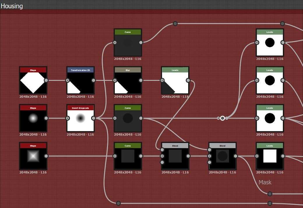
First I built the Housing, it’s a square with a one corner cut off and a cone-shaped hole in the centre, with all the small semiconductors built in.
Next step was to add the 8 contacts to the housing, these will be soldered to the PCB in the Main-Graph. I used the same technique for the soldering, as I did for the resistors, since this technique worked even better on the small connectors.

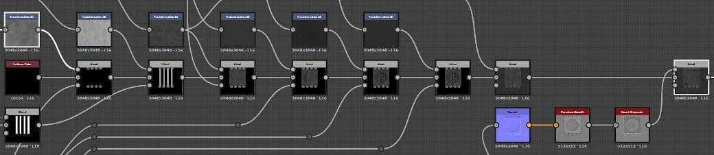
The interesting part was to get the different Layers of the inner LED right. A RGBW-LED-Chip is made of different semiconductors and phosphoric layers, connected with two bonding wires to emit light of a specific wave-length.

I built all the single shapes by using a ton of Transform 2D-Nodes keeping them separated as long as possible, because I need them later as masks for the different materials. To create the Height-Map I used Levels-Nodes and set the right Out-High-Value to blend them all together with Max/Lighten.

For the bonding wires, I used a rectangular shape, added two Ridged Bell-Shapes to the ends, where they are connected to the semiconductors. I multiplied the blended wire with a Gradient Linear 2 to create a round height and finally warped the result with a Perlin Noise to break the uniform appearance.

For the color and roughness of the different parts of the LED I used the technique I already used for the resistors. I built materials for all the different parts and blended them together using the masks I created with the Height-Map.

I also used that little trick with the Curvature Smooth for the overall roughness.
For the Colour-Map I used the same masks as for the roughness, to keep the materials consistent.

The Metallic-Map was a little more complicated as to know which parts are metals and what parts are dielectrics. So not all the created masks could be used, because of other parts covering or overlaying them and so they are not metallic anymore.

As with all the other subgraphs I added some scratches and damage to the Chip, so I could expose these parameters as well. Additional to the Edge-Damage and Scratches-Amount I created two parameters to control the color and intensity of the emitted light.

Once the standard-maps were all created, I finally could play around with the emissive part of the material. For this I searched for some references, how the light inside the LED-Chip was really emitted. I found out that it’s just a little spot, right where the bonding-wires meet, where the LED emits light, the rest is just spill light inside the chip's housing.

To create the emissive layer as realistic as possible, I separated the hotspots from the spill lighting component of the chip.

I created four little spots, with a Thorn-Shape applied a very steep almost exponential curve to it, so the hotspot is really just a few pixels and has a steep but visible falloff as masks for the Blend-Nodes.

To create the spill lighting effect I used the mask from the hole, blurred it a little bit and subtracted a Gaussian-Shape. So I got the reflections of the sloped sides a little more intense and used that as a mask for the colour-blending. For the white component of the chip, I used the Blackbody-Node as colour input. This node lets you set a colour temperature in kelvin as a colour (in the case of this chip it’s around 2900K - warm white)

Because I exposed the color as a parameter, I wanted to have a realistic ratio of the brightness of the different colors. I split the Color-Value into its three components and used these as the output-value of three different Uniform Color-Nodes.

To blend everything together in the main-graph I started with the PCB-Graph, then added the resistors and the LED-Chips.

Since I already packed the resistors into an 4x2 atlas I built a small Utility-Node to split the material-atlas and output the resistors in the right order and at the right position of the stripe. The only exposed parameter is the stripe-number from 1 to 7 (top to bottom).

For the LED-Chips I created a similar graph, which takes the LED-Subgraph as an Material-Input and outputs the LED at the right position. For this I exposed two parameters, X- and Y-Position.

After the material was finished I tried all the parameters and iterated through all the graphs. There was this point, where I wanted to do a colour-gradient over the whole stripe, which was a little bit annoying to set 42 colours by hand. I created another Utility-Graph which takes an Input-Pattern of 6x7 colours and outputs the corresponding colour-values, which could be fed back into the LED-Graph to set the colour by a simple pattern. I also wanted the user to have the possibility to set specific values, so I exposed a Colour-Mode parameter which switches between the Input-Value and the Input-Pattern.
As I said at the beginning, this material was meant to advance my skills working with Substance Designer. It took almost four weeks to create it, because every iteration brought new challenges. Even now, when I went through the graphs to write the breakdown I rebuilt some parts of the material.

I challenged myself one last time and created an option for the LED-Chip, which can have a closed cap. This was a very tricky part, because I wanted to keep the height information of the inner LED by actually having no real height or normal information. So I tried a lot of things and ended up using an Ambient Occlusion-Node multiplied into the Colour-Map. I used the cap as a mask, to remove all the information from the Height-, Metallic- and Roughness-Map to “fake” some height inside the LED-Chip.


If you have any questions on the breakdown, the material or just want to get in touch, don’t hesitate to contact me. I’m looking forward to reading your feedback, questions and comments!